
News Releases
Konica Minolta Starts Polishing Glass Lenses in Hachioji, Tokyo, for Optical Components Used in Semiconductor Inspection Equipment
Making Steady Progress in Initiative to Increase the Production Capacity
April 22, 2026
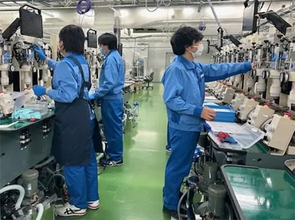
Tokyo (April 22, 2026) - Konica Minolta, Inc. (Konica Minolta) today announced that the Company has established a new process to polish lenses for semiconductor inspection equipment at Tokyo site Hachioji and started operations at the end of March 2026 as part of its initiative to expand the optical components business for semiconductor inspection equipment. The Company will enhance supply stability and meet growing demand by reinforcing the production system at Tokyo site Hachioji in addition to that of Osaka Sayama site, which is the main production site.
Background to Expansion of Production Capacity
Konica Minolta develops and manufactures optical components for semiconductor inspection equipment, which is indispensable for semiconductor manufacturing processes. In recent years, even greater performance is required due to the growing demand for semiconductors for AI and data centers and ever-increasing semiconductor performance.
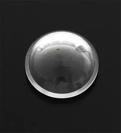
Konica Minolta’s optical components are among the key elements determining the inspection system performance, as lens accuracy and quality directly impact inspection results. Konica Minolta, which regards the optical components business for semiconductor inspection equipment as a growth area, has been developing a system to increase the production capacity in anticipation of future demand growth.
Previously, optical components for semiconductor inspection equipment were manufactured at Osaka Sayama site. To increase the production capacity, Konica Minolta studied the feasibility of scaling up the lens polishing process to strengthen the production system and support business growth, and has now set up the lens polishing process at Tokyo site Hachioji, which is the existing development and production site for the optical components business, and started operations. Lenses polished at Tokyo site Hachioji are transported to Osaka Sayama site and eventually assembled into lens units for shipment.
semiconductor
inspection systems
Tokyo site Hachioji
Future Plan
Konica Minolta will accelerate growth in its optical components business for the semiconductor field by implementing a phased expansion of lens polishing capacity at Tokyo site Hachioji, while strengthening collaboration with Osaka Sayama site. Through this enhancement, Konica Minolta’s lens production capacity for semiconductor inspection equipment is expected to reach 2.6-fold in FY2026 compared to FY2024. In response to expected growth in demand for optical components used in semiconductor inspection system, the Company aims to rapidly expand its business in a sustainable manner by offering products that meet customers’ exacting requirements and building a stable supply system.
Features of the Polishing Process at Tokyo Site Hachioji
Rapid Process Setup by Harnessing the Technological Foundation
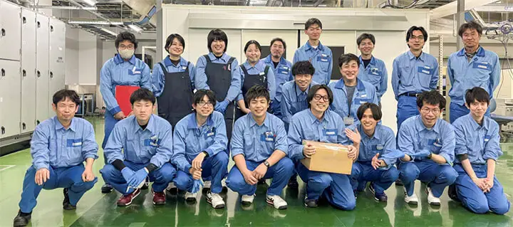
Tokyo site Hachioji is an existing development and production site, where mold machining and evaluation technologies have been refined through the manufacture of pickup lenses for optical discs. This enabled the lens polishing process to be set up quickly by using the accumulated technological foundation and human resources as well as the environment that allows close collaboration with respective business units and the Corporate Technology Development Headquarters, which conducts R&D.
Increased Machining Efficiency by Using DX
Konica Minolta has been improving efficiency by streamlining the machining process by quantifying and standardizing the expertise of skilled technicians through the introduction of NC machines and the use of DX.